
Truth table for jk flip flop :The JK Flip Flop is a pair of flip flops designed by JK
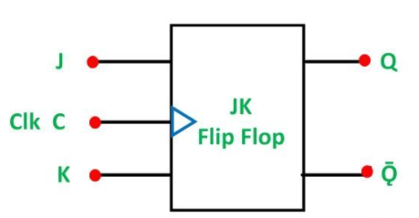
What is JK Flip Flop ?
The JK Flip Flop is the most popular type of flip flop. It is regarded as a universal flip-flop circuit. The JK Flip Flop operates in the same way as the RS flip-flop, with the identical SET and RESET inputs.

When the J and K inputs are both LOW, the JK Flip-flop behaves similarly to the SR Flip-flop, but there is no change in state.
The basic S-R NAND flip-flop circuit offers a lot of benefits and applications in sequential logic circuits, but it has two major switching issues.
- Always avoid the Set= 0 and Reset=0 conditions (S= R = 0).
- If the state of Set or Reset changes when the enable (EN) input is high, the latching operation may not be proper.
The JK Flip Flop eliminates the SR Flip Flop’s two flaws.
In digital circuits, the JK flip flop is one of the most often used flip flops. The JK flip flop is a global flip flop that accepts two inputs: ‘J’ and ‘K.’ The reduced truncated letters for Set and Reset in the SR flip flop are ‘S’ and ‘R,’ however J and K are not. The J and K are stand-alone letters that were chosen to set the flip flop design apart from others.
The JK Flip Flop is a gated SR flip-flop with a clock input circuitry added to it. When both inputs are set to 1, an invalid or illegal output state occurs, which can be avoided by using a clock input circuit. As a result, the JK flip-flop has four input combinations: 1, 0, “no change,” and “toggle.” Except for the inclusion of a clock input, the JK flip flop has the same symbol as the SR Bistable Latch.
flip flop jk truth table is an improvement on the SR flip-flop where S=R=1 is not a problem.
The simple NAND gate RS flip-flop has two major flaws.
To begin with, the condition where S = 0 and R = 0 should be avoided.
Second, if the state of S or R changes while the enabled input is high, the right latching operation is not performed.
To address these two issues with the RS Flip-Flop, the JK Flip Flop was created.
The JK Flip Flop is just a gated RS flip flop with clock input circuitry added. The invalid situation occurs when both inputs S and R are equal to logic “1.”
jk flip flop truth table

jk flip flop truth table
The JK flip flop operates in the same manner as the SR flip flop. The JK flip flop bears the letters ‘J’ and ‘K’ instead of ‘S’ and ‘R.’ The main difference between a JK flip flop and an SR flip flop is that when both inputs of an SR flip flop are set to 1, the circuit creates invalid states as outputs, but in the case of a JK flip flop, there are no invalid states even when both ‘J’ and ‘K’ flip flops are set to 1.flip flop jk truth table
truth table of jk flip flop with clock
| J | K | Q | Q’ |
| 0 | 0 | 0 | 0 |
| 0 | 1 | 0 | 0 |
| 1 | 0 | 0 | 1 |
| 1 | 1 | 0 | 1 |
| 0 | 0 | 1 | 1 |
| 0 | 1 | 1 | 0 |
| 1 | 0 | 1 | 1 |
| 1 | 1 | 1 | 0 |
jk flip flop truth table
SR Flip Flop
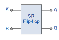
The SR flip flop is a bistable 1-bit memory device with two inputs, SET and RESET. The RESET input ‘R’ resets the device or produces the output 0. The SET input ‘S’ sets the device or produces the output 1, and the RESET input ‘S’ sets the device or produces the output 0. S and R are the labels for the SET and RESET inputs, respectively.
The “Set-Reset” flip flop is known as the SR flip flop. From the present state with an output ‘Q,’ the reset input is utilised to return the flip flop to its original state. This output is determined by the set and reset conditions, which are either “0” or “1” logic levels.
Sequential SR Flip flop Logic’s Classification
Bifurcated latches and flip-flops are the essential building blocks of sequential logic circuits, much as regular logic gates are for combinational circuits. Simple edge-triggered flip-flops or more complicated sequential circuits such as store registers, shift registers, memory devices, or counters can be built using sequential logic circuits. Sequential logic circuits can be split into three primary categories in either case:
- Event-driven circuits — asynchronous circuits that change state as soon as they are turned on.
- Clock-driven circuits are synchronous circuits that are timed to a specific clock signal.
- Pulse Driven – a hybrid of the first two that reacts to triggering pulses.
Truth table for SR flip flop
| S | R | Q | Q’ |
| 0 | 0 | 0 | 1 |
| 0 | 1 | 0 | 1 |
| 1 | 0 | 1 | 0 |
| 1 | 1 | ∞ | ∞ |
In the second stable condition, output Q’ is 0 and output Q is 1. R = 1 and S = 0 give it away. The NAND gate ‘X’ has a 0 as one of its inputs and a 1 as its output Q. As input B, output Q is faded to NAND gate Y. As a result, both inputs of NAND gate Y are set to 1, and Q’ = 0.
If the input S is changed to 0 but the input R remains 1, the output Q’ will be 0 and the state will remain unchanged. As a result, the flip flop circuit’s reset state has been latched, and the set/reset actions are defined in the truth table below:
We can see from the truth table above that when the set ‘S’ and reset ‘R’ inputs are both set to 1, the outputs Q and Q’ are either 1 or 0. Before the input condition exists, these outputs are dependent on the input state S or R. As a result, when the inputs are 1, the outputs’ statuses stay unaltered.
Related posts